As the global semiconductor industry continues to expand rapidly, silicon wafers have become the essential foundation behind virtually all modern electronics—from smartphones and electric vehicles to AI systems and IoT devices.
Yet many businesses still struggle with:
- Understanding what a silicon wafer truly is
- Identifying the right specifications for their application
- And most critically: how to source wafers quickly without waiting months for production lead time
This guide provides a complete overview—and more importantly—introduces a ready-to-ship silicon wafer solution from Kanetora, helping you accelerate your projects immediately.
1. What is a Silicon Wafer?
A silicon wafer is a thin, flat slice of ultra-pure single-crystal silicon, used as a substrate for manufacturing integrated circuits (ICs), sensors, and other semiconductor devices.
Key characteristics:
- Ultra-high purity (up to 99.9999999%)
- Mirror-polished surface
- Precisely controlled electrical conductivity through doping
👉 Simply put:
Silicon wafers are the foundation on which the entire electronics industry is built.
2. How are Silicon Wafers Manufactured?
The production of silicon wafers involves several highly controlled steps:
- Silicon purification from quartz (SiO₂)
- Crystal growth (Czochralski method – CZ)
- Wafer slicing
- Grinding, polishing, and surface treatment
- Quality inspection (defects, resistivity, flatness)
👉 Even minor variations in this process can significantly impact chip yield and performance.
3. Types of Silicon Wafers
By grade:
- Prime wafers – for semiconductor production
- Test wafers – for R&D and training
- Reclaim wafers – recycled and reused
By structure:
- Standard silicon wafers
- SOI wafers (Silicon-on-Insulator)
- Epitaxial (Epi) wafers
By size:
- 2” – 4” – 6” (150 mm)
- 8” (200 mm)
- 12” (300 mm, advanced fabs)
4. Applications of Silicon Wafers
Silicon wafers are widely used across industries:
🔹 Semiconductor industry
- ICs, CPUs, GPUs
- Memory chips, AI processors
🔹 Electronics manufacturing
- Sensors and MEMS devices
- Automotive electronics
🔹 Energy sector
- Solar cells (photovoltaics)
🔹 Research & education
- Universities and R&D labs
- Material science development
5. Key Specifications When Selecting a Wafer
Choosing the right wafer is critical for performance and yield.
Important parameters:
- Crystal orientation: <100>, <111>
- Type/Dopant: P-type (Boron), N-type
- Resistivity
- Diameter & thickness
- TTV (Total Thickness Variation)
- Bow / Warp
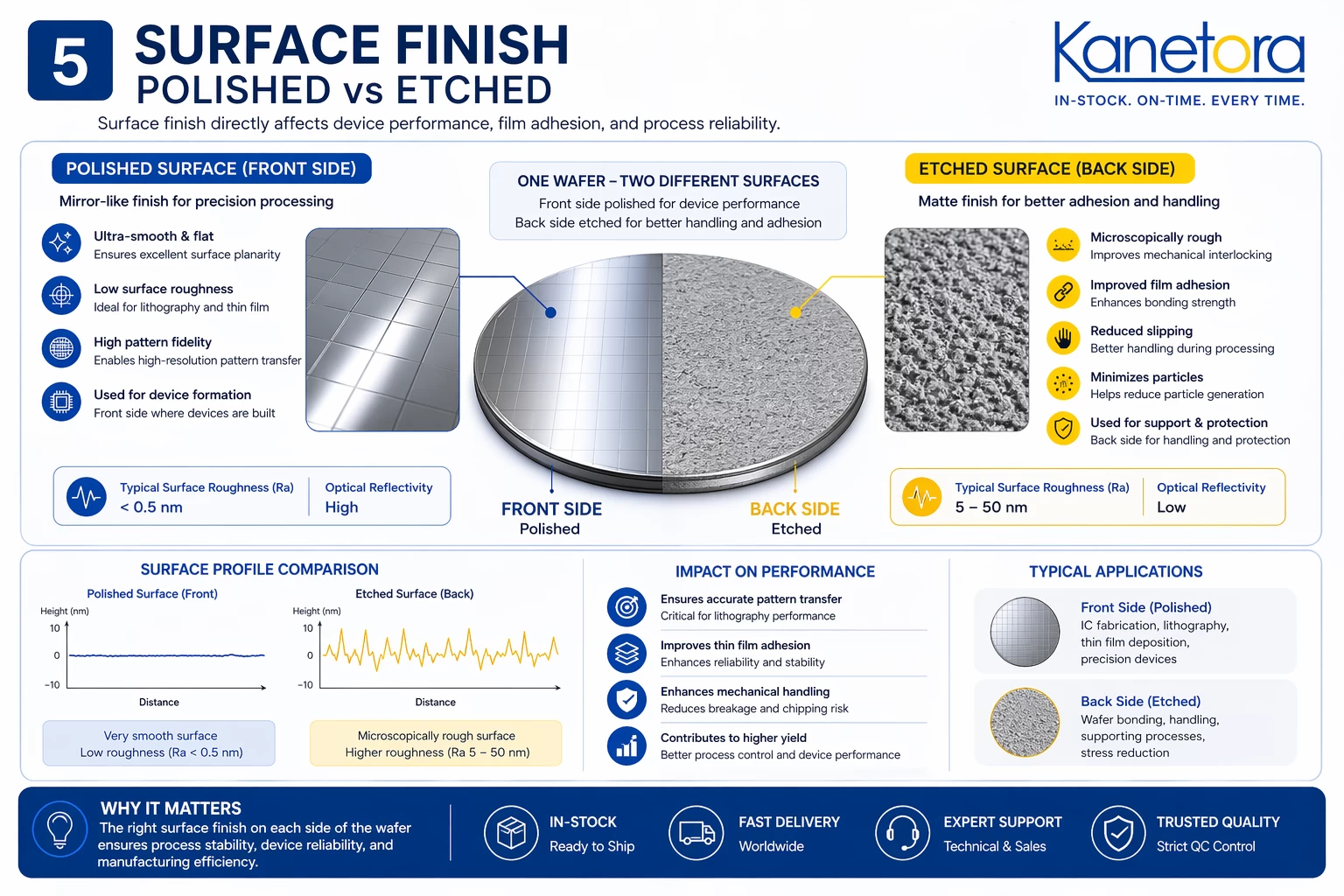
- Surface finish (polished, etched)
6. Real Case: 6-inch P-type <100> Wafer – Available in Kanetora Stock
Based on Kanetora’s actual Technical Data Sheet :
Key specifications:
- Diameter: 150 mm (6 inch)
- Orientation: <100> ±1°
- Type: P-type
- Dopant: Boron
- Resistivity: 1 – 100 Ω·cm
- Thickness: 675 ± 25 µm
- TTV: <10 µm
- Bow/Warp: <40 µm
- Surface: Front polished – Back etched
- Particles: <10 ea/pc @ ≥0.3 µm
- Packaging: 25 wafers per cassette
👉 This configuration is widely used for:
- Semiconductor R&D
- MEMS fabrication
- University training programs
7. Market Trend: From Buying Wafers to Buying Solutions
A major shift is happening in the semiconductor supply chain:
👉 Businesses are no longer just looking for low-cost wafers
👉 They need availability, speed, and technical support
Common challenges:
- Long lead times (6–12 weeks or more)
- High minimum order quantities (MOQ)
- Limited flexibility for R&D needs
8. CTA – Kanetora’s In-Stock Silicon Wafer Solution
🚀 Kanetora provides ready-to-ship silicon wafers with real operational advantages:
✔ IN-STOCK AVAILABILITY
- 6-inch (150 mm) P-type <100> wafers
- Standardized, production-ready specifications
- Immediate availability
✔ NO LONG LEAD TIMES
- Reduce waiting time from months → days
- Ideal for urgent projects, R&D, and pilot production
✔ TECHNICAL SUPPORT
- Expert consultation on wafer selection
- Support for enterprises, universities, and labs
✔ GLOBAL DELIVERY
- Serving Vietnam and international partners
- Flexible quantities based on your needs
👉 Contact Kanetora Today
If you are:
- Developing semiconductor or electronic products
- Looking for wafers for R&D or training
- Or trying to shorten your project timeline
👉 Contact Kanetora’s Silicon Wafer specialists today for fast, reliable support and immediate supply.