

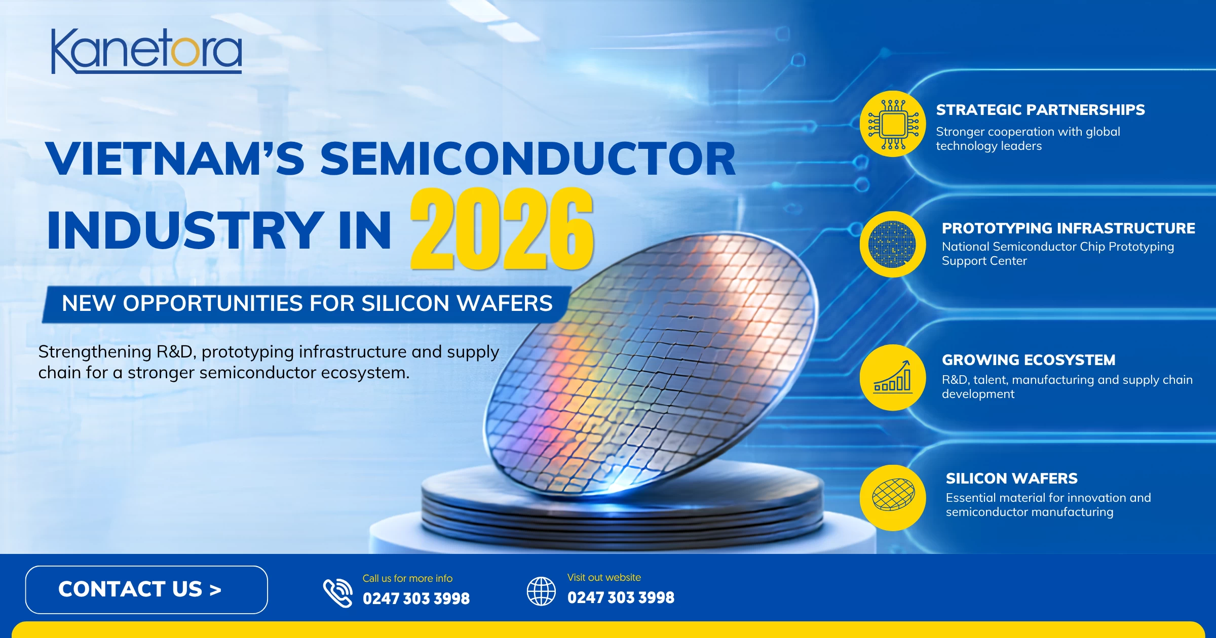
Vietnam’s semiconductor industry is entering a new stage of development.
While the country has traditionally been recognised for electronics manufacturing, chip design, assembly, packaging and testing, recent developments indicate a broader shift towards research and development, chip prototyping, technology commercialisation, domestic manufacturing capabilities and semiconductor material supply.
In July 2026, Vietnam encouraged Qualcomm to expand its cooperation in artificial intelligence, semiconductors and research and development. The two sides discussed workforce training, R&D capacity, technology commercialisation and stronger connections between research institutions, innovative businesses and industry.
Another major development came in June 2026, when Vietnam officially launched its first National Semiconductor Chip Prototyping Support Center. The facility is expected to strengthen the country’s research and prototyping infrastructure, support domestic enterprises and help Vietnamese organisations participate more deeply in the global semiconductor value chain.
Together, these developments create opportunities not only for chip-design companies, but also for suppliers of silicon wafers, semiconductor substrates, laboratory materials, prototyping equipment and technical supply-chain solutions.
Key Takeaways
Vietnam’s semiconductor development is currently centred on four major priorities:
- Improving semiconductor-related policies and investment incentives.
- Expanding cooperation with international technology corporations.
- Developing domestic research, prototyping and manufacturing infrastructure.
- Building a workforce and local supply chain for semiconductor materials and equipment.
Silicon wafers play a foundational role in this ecosystem. As Vietnam establishes more semiconductor laboratories, training programmes, prototyping centres and manufacturing projects, demand for wafers with specific diameters, crystal orientations, doping types, resistivity levels and surface finishes is expected to become increasingly specialised.
Two Recent Developments Shaping Vietnam’s Semiconductor Industry
Vietnam Encourages Qualcomm to Expand Semiconductor and R&D Cooperation
During a meeting held in Hanoi on 17 July 2026, Vietnam’s Ministry of Science and Technology encouraged Qualcomm to broaden its cooperation in artificial intelligence, semiconductors and research and development.
The two sides discussed several areas of potential cooperation, including:
- Semiconductor and AI workforce development.
- R&D capacity building.
- Commercialisation of research outcomes.
- Support for Vietnamese technology companies and startups.
- Stronger connections between universities, research institutions and industry.
Qualcomm also expressed interest in expanding partnerships with Vietnamese technology companies, particularly in AI and semiconductors.
This direction is important because a sustainable semiconductor ecosystem requires more than foreign investment or individual chip-design projects. It requires a connected development pathway:
Research → prototyping → testing → commercialisation → industrial application
As this pathway becomes more established, universities, laboratories, startups and technology companies will require more reliable access to semiconductor wafers for education, process development, MEMS research, sensors, power electronics and other advanced applications.
Vietnam Launches Its First National Semiconductor Chip Prototyping Support Center
On 26 June 2026, Vietnam officially launched its first National Semiconductor Chip Prototyping Support Center.
The centre is intended to provide infrastructure that helps connect chip design with practical prototyping and testing. It is also expected to support Vietnamese researchers and enterprises in turning designs and research outcomes into physical semiconductor products.
This development addresses an important gap in Vietnam’s semiconductor ecosystem.
Designing a chip through electronic design automation software is only one stage of the process. Researchers and businesses also need access to wafer processing, prototyping, packaging, testing and technical validation before a design can move towards commercial production.
The prototyping centre may therefore increase demand for:
- Test wafers for process development.
- Dummy wafers for equipment setup and calibration.
- Polished wafers for laboratory and fabrication processes.
- Epitaxial wafers for devices requiring controlled doping layers.
- SOI wafers for MEMS, RF and low-power applications.
- Compound semiconductor wafers for power and high-frequency technologies.
Vietnam Is Gradually Completing Its Semiconductor Value Chain
Vietnam has built a significant electronics and semiconductor presence through chip design, assembly, packaging and testing activities.
However, wafer fabrication remains one of the most complex and capital-intensive stages of the semiconductor value chain.
A major step was taken in early 2026 when Viettel began developing Vietnam’s first domestic semiconductor chip manufacturing plant at Hoa Lac High-Tech Park. The project is expected to support domestic manufacturing capabilities, practical workforce training and greater technological autonomy.
At the same time, Intel has continued discussions with the Vietnamese Government on expanding high-tech investment, supporting chip prototyping infrastructure, developing human resources and strengthening the domestic semiconductor ecosystem.
Together, these initiatives show that Vietnam is gradually moving beyond individual design, packaging or testing projects towards a more integrated semiconductor ecosystem.
What Is the Vietnamese Government’s Semiconductor Development Strategy?
National Semiconductor Strategy Through 2030, with a Vision to 2050
Vietnam’s semiconductor industry development strategy was approved under Decision No. 1018/QD-TTg in September 2024.
For the 2024–2030 period, Vietnam aims to build fundamental capabilities in semiconductor research, design, production, packaging and testing while becoming a global centre for semiconductor human resources.
The strategy sets targets that include:
- At least 100 chip-design companies.
- One small-scale semiconductor fabrication plant.
- Ten semiconductor packaging and testing facilities.
- More than 50,000 engineers and graduates serving the semiconductor industry.
- Annual semiconductor industry revenue exceeding USD 25 billion by 2030.
- Domestic value added representing approximately 10–15% of industry revenue.
The longer-term roadmap aims to expand domestic design, manufacturing, packaging and testing capacity while gradually enabling Vietnamese organisations to participate in higher-value stages of the global semiconductor chain.
This policy direction combines several elements:
- Attraction of foreign direct investment.
- Development of Vietnamese semiconductor enterprises.
- Research and technology transfer.
- Workforce training.
- Infrastructure and laboratory development.
- Local supply-chain participation.
Policy Support for Semiconductor Materials and Equipment
Vietnam has also introduced legal and investment frameworks supporting digital technology and semiconductor development.
The policy direction covers semiconductor materials, manufacturing equipment, research infrastructure and other essential elements of the value chain. These measures are intended to improve the investment environment while supporting the development of domestic semiconductor capabilities.
Material groups relevant to semiconductor development include:
- High-purity silicon and polysilicon.
- Semiconductor wafers.
- Silicon carbide, or SiC.
- Gallium nitride, or GaN.
- Gallium arsenide, or GaAs.
- Indium phosphide, or InP.
- Chemicals and consumables used in cleaning, photolithography and wafer processing.
The inclusion of wafers and semiconductor materials in Vietnam’s policy direction is significant. It suggests that the country is not only seeking to attract chip-design and manufacturing projects, but also to build a broader supporting supply chain.
What Is a Silicon Wafer?
A silicon wafer is a thin, precisely processed slice of ultra-pure single-crystal silicon. It is used as a substrate for manufacturing integrated circuits, sensors, MEMS devices, power components and many other semiconductor products.
During semiconductor manufacturing, multiple layers and microscopic structures are created on the wafer surface through processes such as:
- Oxidation.
- Thin-film deposition.
- Photolithography.
- Etching.
- Ion implantation or doping.
- Cleaning.
- Inspection and metrology.
A silicon wafer is therefore not a finished chip. It is the physical foundation on which semiconductor devices are fabricated.
Readers seeking a complete technical introduction can explore Kanetora’s guide: What Is a Silicon Wafer? Applications in Semiconductor and Industrial Manufacturing.
Important Specifications When Selecting Silicon Wafers
Selecting the correct wafer requires more than choosing a diameter.
Key technical specifications include:
Wafer Diameter
Common wafer sizes include:
- 2 inches.
- 3 inches.
- 4 inches.
- 6 inches or 150 mm.
- 8 inches or 200 mm.
- 12 inches or 300 mm.
Smaller wafers are frequently used for education, specialised research and legacy processes, while larger wafers are commonly associated with industrial semiconductor manufacturing.
Crystal Orientation
Typical orientations include:
<100><110><111>
The appropriate orientation depends on the fabrication process, device design, etching behaviour and mechanical requirements.
Conductivity Type and Dopant
Silicon wafers may be supplied as:
- P-type, commonly doped with boron.
- N-type, commonly doped with phosphorus.
- Intrinsic or high-resistivity silicon.
The dopant and resistivity affect the wafer’s electrical characteristics and suitability for different devices.
Surface Finish
Available finishes may include:
- As-cut.
- Lapped.
- Etched.
- Single-side polished, or SSP.
- Double-side polished, or DSP.
Surface quality affects photolithography, thin-film deposition, bonding, metrology and overall process stability.
Thickness, TTV, Bow and Warp
Thickness tolerance, total thickness variation, bow and warp influence equipment compatibility, handling stability and process uniformity.
For R&D projects, these factors should be specified carefully, especially when wafers will be used in spin coating, lithography, bonding or precision measurement.
Types of Wafers Supporting Semiconductor Development
Bare Silicon Wafers
Bare silicon wafers are commonly used for process development, research, equipment calibration and semiconductor manufacturing.
They may be classified as:
- Dummy wafers: Used for equipment setup, handling tests and process optimisation.
- Test wafers: Used for process trials, development and pilot production.
- Prime wafers: Produced with stricter surface and defect requirements for critical fabrication processes.
Kanetora provides CZ and FZ bare silicon wafers in multiple sizes, dopant options and surface finishes. Explore Bare Silicon Wafers.
Epitaxial Wafers
Epitaxial, or EPI, wafers feature one or more precisely controlled crystalline layers grown on a substrate.
They are suitable for applications requiring:
- Controlled doping profiles.
- High-performance power devices.
- RF components.
- Logic devices.
- Improved electrical characteristics.
Kanetora supplies EPI wafers with configurable layer thickness, resistivity, orientation and substrate options. Explore EPI Wafers.
SOI Wafers
Silicon-on-insulator wafers contain a thin silicon device layer separated from the handle wafer by an insulating oxide layer.
SOI wafers offer advantages such as:
- Improved electrical isolation.
- Lower parasitic capacitance.
- Reduced power consumption.
- Strong performance in RF and low-power devices.
- Compatibility with selected MEMS applications.
Explore Kanetora’s SOI Wafer Solutions.
Compound Semiconductor Wafers
Compound semiconductor materials such as GaN and SiC are increasingly important for applications that require high voltage, high frequency, high efficiency or operation under demanding conditions.
Typical applications include:
- Power electronics.
- Electric vehicles and charging infrastructure.
- RF communication.
- Optoelectronics.
- Industrial power systems.
- Advanced sensing technologies.
Explore Compound Semiconductor Wafers.
Where Will Silicon Wafer Demand Grow in Vietnam?
Semiconductor Research and Education
Vietnam’s target of developing a large semiconductor workforce will require more practical training facilities.
Universities and research laboratories need wafers for:
- Photolithography training.
- Thin-film deposition.
- Wet and dry etching.
- Surface characterisation.
- Semiconductor device fabrication.
- MEMS and sensor development.
For many of these applications, test wafers, polished wafers and customised wafers in smaller quantities can be more suitable than high-volume production-grade orders.
Chip Prototyping and Process Development
The launch of the National Semiconductor Chip Prototyping Support Center may increase the number of projects moving from design into practical process validation.
These projects may require:
- Prime wafers for critical fabrication steps.
- Test wafers for pilot processes.
- Dummy wafers for calibration.
- EPI wafers for controlled device structures.
- Specialised substrates for experimental designs.
MEMS, Sensors and IoT Devices
Silicon and SOI wafers are widely used in microelectromechanical systems, including:
- Pressure sensors.
- Accelerometers.
- Microphones.
- Biomedical devices.
- Industrial sensors.
- IoT components.
As Vietnam develops smart manufacturing, automation, robotics and connected devices, demand for materials supporting MEMS and sensor development may also expand.
Power Electronics, RF and Energy Technologies
GaN, SiC, EPI and SOI wafers support many emerging applications, including:
- Electric-vehicle power systems.
- Charging stations.
- Renewable-energy inverters.
- Telecommunications equipment.
- Aerospace and satellite technologies.
- Industrial motor control.
- High-frequency communication devices.
The development of AI, 5G, IoT and advanced electronics is therefore likely to create demand for both conventional silicon wafers and compound semiconductor materials.
Kanetora’s Silicon Wafer Solutions
Kanetora focuses on supplying semiconductor wafers for research, education, process development and industrial applications.
Its wafer portfolio includes:
- Bare silicon wafers.
- Dummy wafers.
- Test wafers.
- Prime wafers.
- Polished wafers.
- Epitaxial wafers.
- SOI wafers.
- GaN and other compound semiconductor wafers.
Kanetora’s corporate profile identifies semiconductor materials as one of the company’s strategic business areas. Its silicon wafer products have been used in laboratory projects, research applications and semiconductor education programmes in Vietnam.
The company supports customers with multiple technical configurations, including:
- Wafer diameters from 2 to 12 inches.
- P-type and N-type options.
- Different crystal orientations.
- Custom resistivity and thickness ranges.
- As-cut, lapped, etched, SSP and DSP surfaces.
- Customised notch, flat and dimensional specifications.
Kanetora’s product portfolio and customisation capabilities are designed to serve requirements ranging from R&D and equipment calibration to pilot-scale and industrial semiconductor processes.
Recommended Internal Links
The article should link naturally to the following English pages:
- Semiconductor Wafer Solutions
- What Is a Silicon Wafer?
- Bare Silicon Wafer
- EPI Wafer
- SOI Wafer
- Compound Semiconductor
- The Role of Silicon Wafers in Semiconductor Manufacturing
- Kanetora Attends EnvisionTech Vietnam 2026
What Should Customers Prepare Before Requesting a Wafer Quotation?
To identify a suitable wafer configuration, buyers should provide:
- Intended application: education, research, calibration, prototyping or production.
- Required wafer diameter.
- Crystal orientation.
- P-type, N-type or intrinsic configuration.
- Dopant requirement.
- Resistivity range.
- Required thickness and tolerance.
- Surface finish: SSP, DSP, etched, lapped or as-cut.
- TTV, bow and warp requirements.
- Required quantity.
- Packaging and cleanliness requirements.
- Target delivery schedule.
Clear specifications help reduce technical mismatches and allow the supplier to identify the most suitable available or customised wafer solution.
Outlook for Vietnam’s Semiconductor and Silicon Wafer Market
Developments in 2026 show that Vietnam’s semiconductor ambitions are moving from strategic planning towards practical implementation.
Cooperation with Qualcomm is strengthening links between research, talent development, innovation and industry. The National Semiconductor Chip Prototyping Support Center provides essential infrastructure for turning chip designs into physical prototypes. Meanwhile, domestic manufacturing projects and cooperation with global technology companies are gradually expanding the country’s capabilities across the semiconductor value chain.
The development process will require sustained investment, highly skilled personnel, advanced equipment and long-term international cooperation.
However, it also creates opportunities for Vietnamese universities, laboratories, technology companies and material suppliers to participate from the early stages of ecosystem development.
As the physical foundation for semiconductor fabrication, silicon wafers will become an increasingly important link in Vietnam’s journey towards a more complete and competitive semiconductor industry.
Frequently Asked Questions
Is a silicon wafer the same as a semiconductor chip?
No. A silicon wafer is the substrate on which semiconductor devices are fabricated. After multiple processing stages, the wafer is divided into individual dies, which are then packaged and tested as semiconductor chips.
What is the difference between silicon and silicone?
Silicon is a chemical element widely used as a semiconductor material. Silicone is a family of synthetic polymers commonly used in sealants, adhesives, medical products and consumer applications.
Which wafers are suitable for semiconductor education and research?
Test wafers, dummy wafers and polished silicon wafers are commonly used in research and education. The appropriate option depends on the laboratory equipment, wafer diameter, surface requirements and intended process.
What is the difference between a dummy wafer and a prime wafer?
A dummy wafer is primarily used for equipment setup, handling tests and process calibration. A prime wafer has stricter surface, flatness and defect-control requirements and is suitable for critical semiconductor fabrication processes.
Does Kanetora provide customised silicon wafer specifications?
Yes. Depending on availability and project requirements, wafer diameter, orientation, conductivity type, dopant, resistivity, thickness, surface finish and other technical parameters can be customised.
What types of semiconductor wafers does Kanetora supply?
Kanetora’s portfolio includes bare silicon wafers, dummy wafers, test wafers, prime wafers, EPI wafers, SOI wafers and compound semiconductor materials such as GaN and SiC-related solutions.