

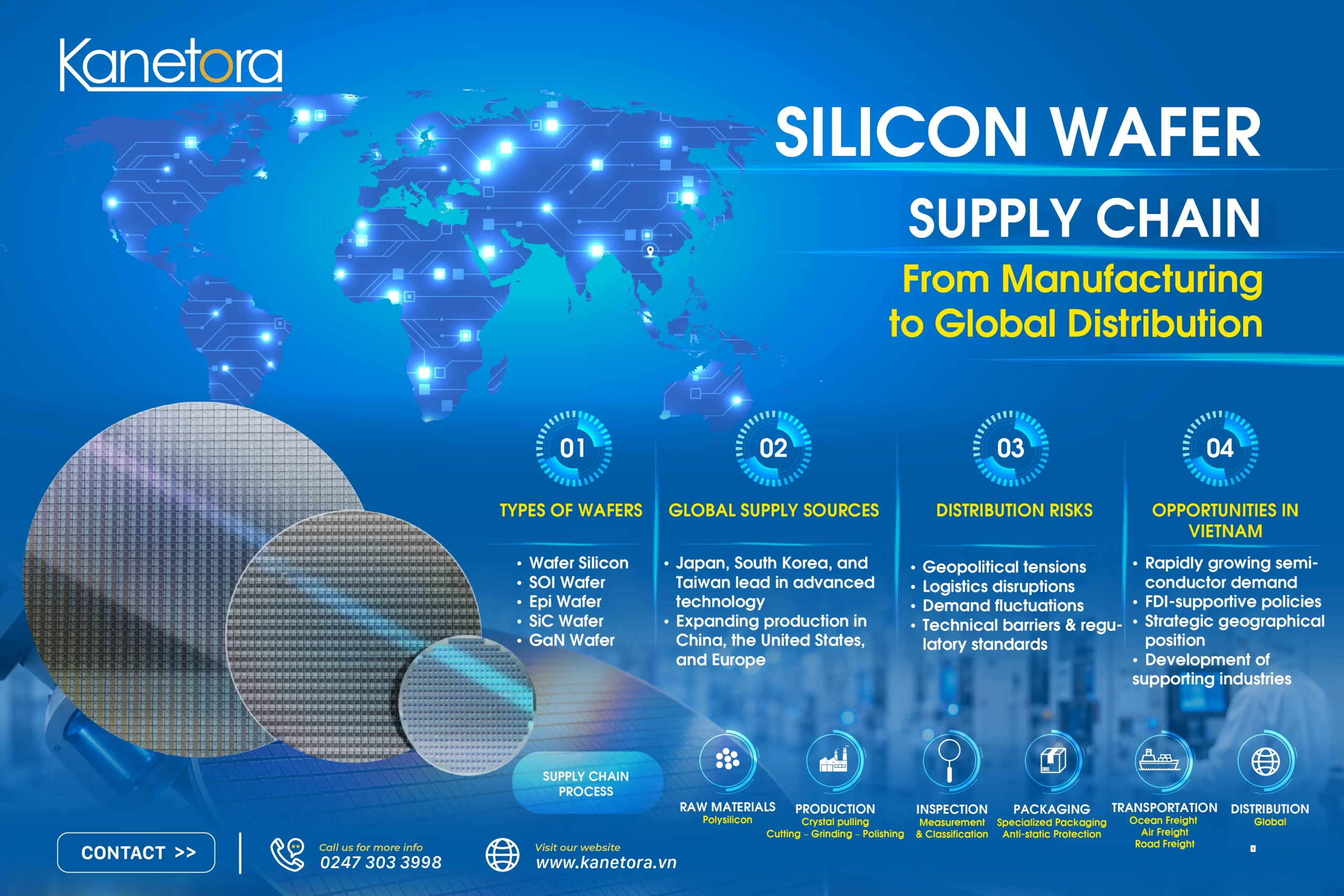
Silicon wafers are critical substrate materials used to manufacture integrated circuits, sensors, power devices, and a wide range of modern electronic components. However, before a wafer reaches a semiconductor fab, research institute, or university laboratory, it must pass through a highly specialized supply chain.
This supply chain covers silicon purification, single-crystal growth, wafer slicing, surface treatment, quality inspection, packaging, and international distribution.
Unlike conventional industrial materials, silicon wafers require extremely high levels of purity, flatness, dimensional accuracy, and electrical consistency. Selecting the right product therefore involves more than identifying a wafer diameter. Buyers must also evaluate technical specifications, manufacturer capabilities, lot traceability, packaging conditions, lead times, and international logistics.
Quick Answer: What Does the Silicon Wafer Supply Chain Include?
The silicon wafer supply chain generally consists of six major stages:
- Sourcing and refining silicon raw materials;
- Producing high-purity polysilicon;
- Growing single-crystal silicon ingots using the CZ or FZ method;
- Slicing, grinding, polishing, and treating wafer surfaces;
- Inspecting, grading, and packing finished wafers;
- Distributing wafers to semiconductor fabs, research institutes, universities, and technology companies.
Not every company or country participates in every stage. The semiconductor ecosystem is highly specialized, with individual economies and manufacturers focusing on particular segments.
According to the OECD, semiconductor production is globally distributed, but many critical inputs and production capabilities remain concentrated in a limited number of regions. This creates supply dependencies and increases the potential impact of production or trade disruptions.
What Is a Silicon Wafer?
A silicon wafer is a thin, flat, circular substrate manufactured from ultra-high-purity single-crystal silicon. It provides the physical foundation on which transistors, integrated circuits, MEMS sensors, power devices, and other semiconductor structures are fabricated.
A wafer can be understood as the technical foundation of a semiconductor chip. During front-end manufacturing, multiple material and circuit layers are built on its surface through processes such as:
- Thermal oxidation;
- Thin-film deposition;
- Photolithography;
- Ion implantation;
- Material etching;
- Surface cleaning;
- Electrical and defect inspection.
For a more detailed introduction, read What Is a Silicon Wafer? Applications in Semiconductor and Industrial Manufacturing.
It is also important to distinguish between three related stages:
- Wafer manufacturing creates the silicon substrate with the required material properties.
- Wafer fabrication or chip fabrication builds integrated circuits on the wafer inside a semiconductor fab.
- Assembly, packaging, and testing take place after the processed wafer is inspected and separated into individual dies.
Understanding these differences helps buyers identify the appropriate material, specification, and supplier for their applications.
How Is the Silicon Wafer Supply Chain Structured?
1. From Silica to Metallurgical-Grade Silicon
The silicon supply chain begins with silica, which is widely found in quartz and quartzite.
According to the U.S. Geological Survey, silica is used to produce silicon metal. A relatively small proportion of this material is subsequently processed into the high-purity silicon required by the semiconductor industry.
Silica is reduced in an electric furnace at high temperatures to produce metallurgical-grade silicon. At this stage, however, the material is not yet pure enough for semiconductor applications.
2. Producing High-Purity Polysilicon
Metallurgical-grade silicon undergoes additional chemical purification to produce ultra-high-purity polysilicon.
Controlling impurities such as metals, carbon, oxygen, and boron is essential during this stage. Even extremely small concentrations of unwanted elements may affect:
- Electrical resistivity;
- Carrier lifetime;
- Crystal quality;
- Defect density;
- Semiconductor device performance.
A reliable polysilicon supply is therefore one of the earliest factors determining the consistency and traceability of finished silicon wafers.
3. Growing Single-Crystal Silicon Ingots
High-purity polysilicon is melted and converted into a single-crystal silicon ingot. Two commonly used crystal-growth methods are Czochralski and Float Zone.
Czochralski Silicon – CZ
In the Czochralski process, a seed crystal is introduced into molten silicon. It is then slowly pulled upward and rotated under tightly controlled conditions, forming a cylindrical single-crystal ingot.
CZ wafers are widely used because they offer:
- Scalable production;
- A broad range of available diameters;
- Competitive production costs;
- Suitability for many mainstream semiconductor applications.
Float Zone Silicon – FZ
The Float Zone method uses a moving molten zone along a silicon rod without relying on a crucible. This enables the material to achieve high purity and relatively low oxygen concentration.
FZ wafers are commonly considered for:
- Power semiconductor devices;
- High-resistivity applications;
- Sensors and detectors;
- Specialized research;
- Devices requiring strict electrical performance.
The choice between CZ and FZ wafers should be based on the electrical requirements, acceptable defect levels, process conditions, availability, and budget of the application.
4. Slicing the Crystal Ingot into Wafers
After crystal growth, the silicon ingot is inspected for crystal orientation, adjusted to the required diameter, and sliced into thin wafers using specialized equipment.
Immediately after slicing, the wafer surface may contain:
- Saw marks;
- Mechanical stress;
- Thickness variation;
- Edge damage;
- Surface roughness.
The wafers therefore undergo edge grinding, beveling, lapping, surface damage removal, and flattening before final polishing.
5. Polishing and Surface Treatment
Depending on the intended application, wafers may be polished on one or both sides. A polished wafer must achieve an exceptionally flat and smooth surface to support photolithography and subsequent semiconductor processes.
Key parameters commonly evaluated include:
- Total Thickness Variation – TTV;
- Bow and warp;
- Surface roughness;
- Defect density;
- Surface cleanliness;
- Electrical resistivity;
- Dopant type and concentration;
- Crystal orientation.
After polishing, the wafers are cleaned to remove particles, metallic contamination, chemical residues, and other surface contaminants.
6. Producing Specialized Wafer Structures
A processed silicon substrate may undergo additional treatments or layer-growth processes to create specialized wafer products.
Polished Wafer
A polished wafer is a silicon substrate with one or both surfaces finished to a precisely controlled level of smoothness and flatness.
It can be used for:
- Semiconductor process development;
- Laboratory research;
- Device fabrication;
- University training;
- Equipment and process evaluation.
Epitaxial Wafer – EPI Wafer
An EPI wafer contains an additional single-crystal silicon layer grown on top of a substrate through epitaxy.
The epitaxial layer allows tighter control over:
- Layer thickness;
- Dopant type;
- Dopant concentration;
- Electrical resistivity;
- Crystal uniformity.
EPI wafers are used in applications such as:
- Power semiconductor devices;
- Analog integrated circuits;
- Sensors;
- Automotive electronics;
- Devices requiring a precisely controlled active layer.
Silicon-On-Insulator Wafer – SOI Wafer
An SOI wafer consists of a thin silicon device layer separated from the bulk substrate by an insulating layer, typically buried oxide.
This structure can provide benefits such as:
- Reduced leakage current;
- Lower parasitic capacitance;
- Improved electrical isolation;
- Lower power consumption;
- Enhanced performance in selected device architectures.
GaN Epi Wafer and Compound Semiconductor Wafers
GaN epi wafers contain a Gallium Nitride epitaxial layer and are commonly considered for applications requiring high power, high frequency, or high-temperature performance.
Typical applications include:
- Power electronics;
- Radio-frequency and telecommunications systems;
- LED technologies;
- Energy converters;
- Fast-charging systems;
- Next-generation energy infrastructure.
Kanetora is developing a semiconductor material portfolio that includes polished wafers, EPI wafers, SOI wafers, and GaN epi wafers for research, education, and technology development.
How Are Silicon Wafers Distributed Globally?
After production and inspection, finished wafers are classified according to their grade, dimensions, electrical properties, surface conditions, and intended use.
They may be supplied directly by the manufacturer or distributed through a specialized semiconductor material supplier.
A typical distribution chain can be summarized as follows:
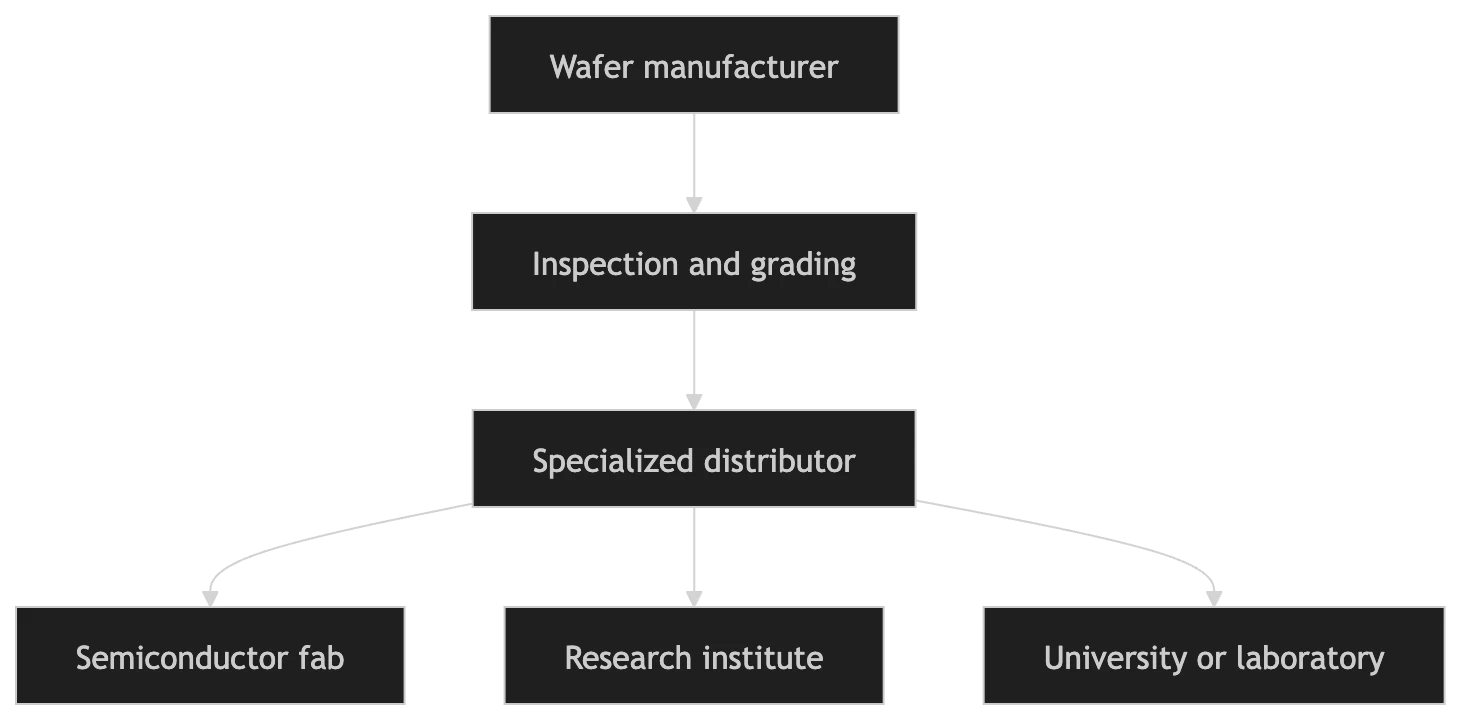
A distributor’s responsibilities can extend beyond product sales. Depending on the project, a specialized wafer distributor may also:
- Collect and clarify technical requirements;
- Match specifications with available sources;
- Source customized wafer configurations;
- Verify documents and product traceability;
- Coordinate specialized packaging and transportation;
- Manage order quantities and delivery schedules;
- Facilitate communication between customers and manufacturers.
This role is particularly important for R&D orders, low-volume requirements, legacy wafer sizes, and customized specifications.
Key Specifications When Sourcing Silicon Wafers
To avoid selecting an incompatible product, buyers should provide at least the following information:
| Specification group | Required information |
|---|---|
| Wafer type | Bare, polished, EPI, SOI, GaN, or another type |
| Growth method | CZ or FZ |
| Diameter | 2, 3, 4, 6, 8, or 12 inches |
| Crystal orientation | Common options include <100> and <111> |
| Conductivity type | P-type or N-type |
| Dopant | Boron, phosphorus, arsenic, or another dopant |
| Resistivity | Required range, normally expressed in Ω·cm |
| Thickness | Nominal thickness and tolerance |
| Surface finish | Single-side polished or double-side polished |
| Grade | Prime, test, monitor, dummy, or research grade |
| Additional requirements | Oxide layer, EPI layer, marking, notch or flat, packaging |
| Quantity | Number of wafers, boxes, or lots |
| Application | R&D, education, equipment testing, or production |
A request stating only “4-inch silicon wafer” is usually insufficient. Two wafers with the same diameter may have completely different applications due to variations in resistivity, dopant, crystal orientation, thickness, or surface condition.
Major Risks in the Global Silicon Wafer Supply Chain
Geographic Concentration of Supply
The semiconductor supply chain is highly specialized across countries, regions, and companies.
OECD analysis shows that semiconductor manufacturing capacity and several critical inputs remain geographically concentrated. The ability to substitute production between facilities is also limited because fabs and material suppliers are designed for particular products, process technologies, and qualification requirements.
A disruption involving energy, natural disasters, logistics, industrial facilities, or trade policies in one region can therefore affect many downstream industries.
Long Lead Times and Technical Qualification
Silicon wafers cannot always be substituted freely between manufacturers. A change in substrate material, crystal-growth process, surface preparation, or wafer specification may require the buyer to repeat part of its qualification process.
Customized wafer products may involve:
- Longer production lead times;
- Specific minimum order quantities;
- Technical drawing or datasheet confirmation;
- Sample production;
- Customer qualification before regular use.
Planning demand early is therefore critical for wafers that are not maintained as standard inventory.
Specification Mismatches
An incorrect resistivity range, crystal orientation, dopant, thickness, or surface condition may make a wafer unsuitable for the customer’s process.
Purchase requirements should therefore be confirmed through a formal specification, datasheet, or technical drawing rather than through a general product name alone.
Packaging and Transportation Risks
Silicon wafers can be affected by:
- Mechanical impact;
- Vibration;
- Particulate contamination;
- Moisture;
- Surface contamination;
- Improper handling.
Wafers should be placed in suitable carriers, cassettes, jars, or specialized boxes with appropriate protection against shock and environmental exposure.
For international shipments, the selected transportation method, packaging configuration, documentation, and customs preparation can directly affect delivery time and product condition.
Technology and Trade Regulations
The semiconductor industry is strongly influenced by export controls, technology restrictions, supply security policies, and international trade relations.
Before placing an order, buyers and suppliers may need to verify:
- Country of origin;
- Expected HS code;
- Export or re-export restrictions;
- Technical documentation;
- End-user information;
- Intended end use;
- Import regulations in the destination market.
How Can Companies Build a More Reliable Wafer Supply?
Standardize the Specification Before Sourcing
A detailed specification improves both technical matching and quotation accuracy.
If the final configuration has not yet been determined, buyers should describe the intended application, process environment, and performance requirements so the supplier can recommend a suitable grade.
Evaluate Both the Product and the Supplier
Price should not be the only purchasing criterion. Buyers should also assess:
- Product origin;
- Quality management practices;
- Availability of technical documentation;
- Lot-to-lot consistency;
- Customization capabilities;
- Sample policy;
- Complaint-handling process;
- Production and delivery lead times.
Develop an Alternative Supply Option
For wafers used regularly, companies should consider evaluating at least one alternative source.
However, a second source must still undergo technical review and qualification. It should not be introduced directly into the process without confirming material and process compatibility.
Forecast Demand and Place Orders Early
Sharing a demand forecast helps suppliers plan raw materials, production schedules, and inventory.
This is especially important for:
- EPI wafers;
- SOI wafers;
- GaN epi wafers;
- FZ wafers;
- High-resistivity wafers;
- Customized specifications.
Maintain Lot-Level Traceability
Lot numbers, certificates, inspection results, and incoming quality data should be recorded for each shipment.
This supports:
- Quality traceability;
- Process comparison;
- Supplier evaluation;
- Root-cause analysis;
- Complaint resolution.
Vietnam’s Opportunities in the Semiconductor and Silicon Wafer Supply Chain
On September 21, 2024, the Vietnamese Government issued Decision No. 1018/QD-TTg, approving the country’s semiconductor industry development strategy through 2030, with a vision toward 2050.
During the initial stage, Vietnam aims to strengthen its capabilities in semiconductor research, design, manufacturing, assembly, packaging, and testing while developing a qualified workforce.
The national human resource development program targets at least 50,000 university-level graduates and professionals across different stages of the semiconductor value chain by 2030.
Vietnam can progressively expand its role in the wafer and semiconductor material supply chain through:
- Semiconductor material distribution;
- Research into materials and fabrication processes;
- Engineering education and training;
- Laboratory and pilot-line development;
- Metrology and inspection;
- Semiconductor assembly, packaging, and testing;
- Electronics manufacturing;
- Connections between international material suppliers and local users.
Instead of attempting to participate in every segment immediately, a practical approach is to build capabilities in suitable areas and expand gradually based on available infrastructure, talent, investment, and market demand.
Kanetora’s Role in the Silicon Wafer Supply Chain
Kanetora focuses on silicon wafer distribution and the connection of semiconductor material sources with research organizations, universities, laboratories, and technology customers in Vietnam and international markets.
The company’s developing portfolio includes:
- Polished wafers;
- EPI wafers;
- SOI wafers;
- GaN epi wafers;
- Wafer solutions for research, education, and technology development.
According to the Kanetora corporate profile, the company aims to support Vietnam’s semiconductor research and education ecosystem while progressively developing its semiconductor material sourcing and distribution capabilities.
Kanetora has supplied silicon wafers for academic research and training activities. Its first silicon wafer order for the School of Materials Science and Engineering at Hanoi University of Science and Technology demonstrated the company’s focus on strengthening collaboration between industry and academia.
Kanetora has also been expanding international cooperation to participate in the global silicon wafer supply chain.
Customers can explore the complete product portfolio on the Kanetora Semiconductor Wafer page.
Frequently Asked Questions About the Silicon Wafer Supply Chain
What are the main stages of the silicon wafer supply chain?
The main stages include silicon raw material processing, polysilicon purification, single-crystal ingot growth, wafer slicing, surface treatment, polishing, inspection, packaging, and distribution.
What is the difference between CZ and FZ wafers?
CZ wafers are widely available, scalable, and suitable for many mainstream semiconductor applications. FZ wafers generally offer high purity and lower oxygen content, making them suitable for high-resistivity, power device, detector, and specialized research applications.
Are prime wafers and test wafers the same?
No. Prime wafers generally meet stricter quality requirements for semiconductor device fabrication. Test, monitor, and dummy wafers are mainly used for equipment setup, process monitoring, training, or non-critical experiments.
Why is a detailed specification required when purchasing wafers?
A specification defines the wafer diameter, crystal orientation, dopant, conductivity type, resistivity, thickness, surface finish, and other technical properties.
Without this information, the supplier cannot accurately determine whether a wafer is compatible with the customer’s process.
Does Vietnam currently manufacture silicon wafers?
Vietnam is developing its semiconductor ecosystem and capabilities across several segments. However, semiconductor material research, wafer distribution, silicon substrate manufacturing, chip fabrication, and semiconductor assembly and testing are different stages with distinct technology and investment requirements.
Claims regarding local wafer manufacturing should therefore be evaluated according to the specific process and production scale involved.
What is Kanetora’s role in the wafer supply chain?
Kanetora focuses on distributing silicon wafers, sourcing materials according to customer specifications, and connecting international wafer sources with customers in research, education, and technology development.
Conclusion
The silicon wafer supply chain is a highly specialized global system that begins with silica and ends at semiconductor fabs, research institutes, universities, and technology laboratories.
Wafer quality depends not only on silicon purity but also on crystal-growth methods, surface treatment, dimensional control, inspection, traceability, packaging, and transportation.
A reliable sourcing strategy must therefore address both technical specifications and supply chain requirements.
As Vietnam advances its semiconductor development strategy, access to suitable wafer materials will support engineering education, scientific research, laboratory development, and the gradual expansion of domestic semiconductor capabilities.
For polished wafers, EPI wafers, SOI wafers, GaN epi wafers, or customized silicon wafer requirements, customers can contact Kanetora with their technical specifications, intended application, and required quantity for sourcing support.
References
- U.S. Geological Survey – Silicon Statistics and Information
- OECD – Mapping the Semiconductor Value Chain
- OECD – The Chip Landscape: Geographical Distribution of Wafer Fabrication Capacity
- Vietnamese Government – Decision No. 1018/QD-TTg
- Ministry of Planning and Investment – Semiconductor Human Resources Development Program