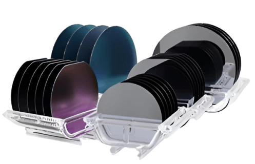
SOI wafers feature a thin layer of silicon on top of an insulating oxide layer, offering superior electrical isolation, reduced parasitic capacitance, and enhanced performance in RF and low-power applications. Kanetora provides tailored SOI wafers for advanced semiconductor needs.
Capability
We are capable of providing customized solutions tailored to your specific project needs. Contact us today to check real-time availability for each specification.
Layer
Item
Min.
Max.
Device Layer (Top)
Crystal Growth Method
CZ, FZ
Diameter
2" – 8"
Thickness
0.05 µm
>300 µm
Tolerance
±5%
Crystal Orientation
(100), (110), (111)
Type / Dopant
P/Boron, N/Phosphorus, Intrinsic
Resistivity
0.001 ohm-cm
>20,000 ohm-cm
Buried Oxide (BOX) Layer
Thickness
0.1 µm
3 µm
Tolerance
±5%
Back Surface
Etched or Polished with Oxide
Handle Layer
Crystal Growth Method
CZ, FZ
Diameter
2" – 8"
Thickness
200 µm
750 µm
Tolerance
±5%
Crystal Orientation
(100), (110), (111)
Type / Dopant
P/Boron, N/Phosphorus, Intrinsic
Resistivity
0.001 ohm-cm
>20,000 ohm-cm
Overall Wafer
TTV
<5 µm
BOW
<20 µm
Lead time
9 – 12 weeks (on average)
Why Choose Kanetora?
At Kanetora, we proudly support our partners in the semiconductor industry with high-quality wafers, a diverse product portfolio, and flexible customization tailored to every technical need.